
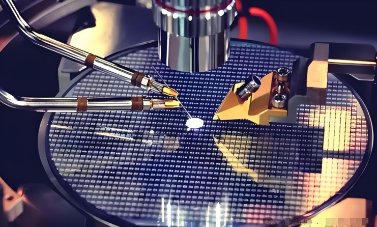
Cutting Carbon in the Fab: Let’s Talk About Drying
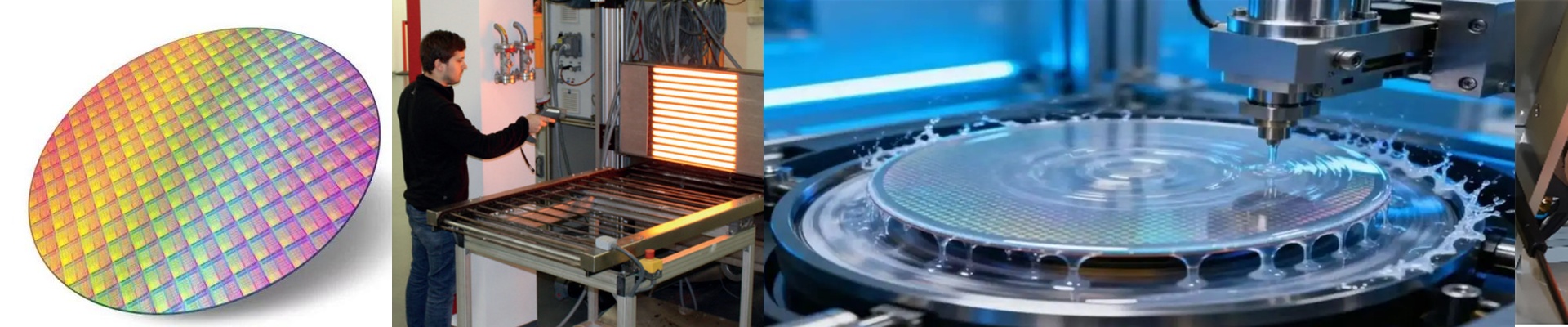
Let’s be honest: semiconductor fabs are absolute energy hogs. A huge chunk of that power disappears into the drying process, where you’re fighting to get moisture off wafers without ruining them with heat or gunk. If you’re trying to hit carbon-neutral goals, you can’t keep doing things the old way. That’s where infrared (IR) heating comes in.
The reality of IR energy audits
Old-school convection drying is basically like trying to heat a whole house just to warm up one plate of food. It’s a waste. IR changes the game because it beams energy straight to the wafer surface. When we go in to audit a drying line, we’re looking for a “spectral match.” Think of it like tuning a radio. Shortwave IR digs deep, while medium-wave sticks to the surface. If the lamp’s peak matches what the wafer actually absorbs, you stop throwing heat into the void.
Shrinking the footprint
Switching to high-density IR lamps does more than just save power—it saves space. These systems ramp up fast. Really fast. You don’t have to leave the machine idling at high temps for hours just to be ready. Plus, with precise IR zoning, you can control the temperature across the wafer perfectly. No more over-processing just to be “safe.”
The trade-offs (because nothing is free)
Now, here’s the catch. High-wattage lamps give you that speed, but they hit your power grid hard. You’ll need to check your electrical panels to make sure they can handle that initial surge without tripping. And then there’s the heat. These lamps getintense. If your cooling fans or heat sinks are mediocre, you’re going to warp your chassis. It’s a real risk if you don’t plan for the airflow. At the end of the day, we care about one thing: kWh per wafer. Replacing those clunky legacy heaters with tuned IR arrays just drops the energy draw. It’s a straightforward way to go green without slowing down your production.